


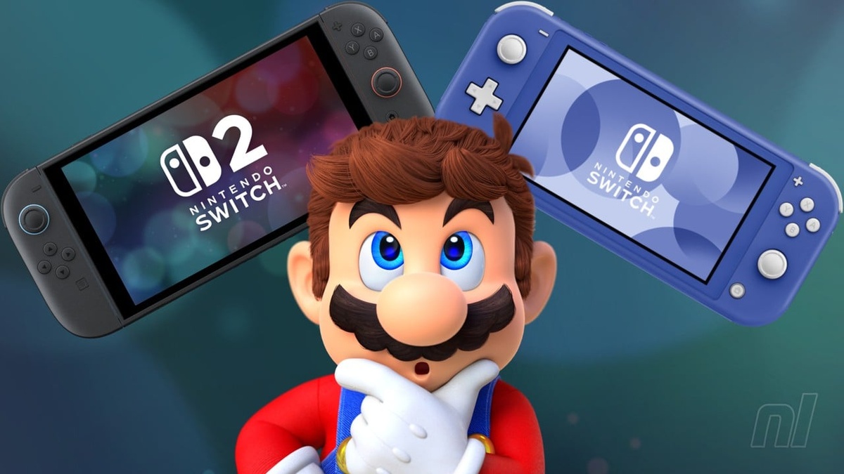
Industry speculation regarding a potential Nintendo Switch 2 Lite has ignited following reports of Samsung’s upcoming semiconductor node, prompting technical analysts to examine whether next-generation silicon can truly support a downsized handheld form factor.
According to reporting from Nintendo Life and semiconductor disclosures, Samsung is preparing its second-generation 8nm process for late 2026, triggering widespread debate regarding handheld efficiency, manufacturing economics, and real-world gaming performance.
| Hardware Metric | Nintendo Switch 2 (Standard T239) | Rumoured Nintendo Switch 2 Lite (8LPU+) | Architectural Node Difference | Portable Gaming Impact |
|---|---|---|---|---|
| Foundry Process Node | Samsung 8nm Custom (8LPP Hybrid) | Samsung 8LPU+ FinFET (2nd-Gen 8nm) | Iterative optical shrink and refinement | Modest thermal reduction without major architectural redesign |
| Processor Power Draw | Estimated 12W – 15W active load | Estimated 10.2W – 12.8W (15% reduction) | 15% power reduction at iso-frequency | Requires active cooling fan and adequate chassis volume |
| Logic Die Area | Baseline T239 monolithic die (~200mm²) | ~8% logic area shrink (~184mm²) | 8% logic and ~10% I/O reduction | Limited physical footprint reduction for compact handheld motherboards |
| DLSS & Tensor Cores | Ampere-derived Tensor cores enabled | Requires identical silicon feature parity | Retains full Tegra T239 feature set | Guarantees complete backwards compatibility across the software ecosystem |
| Form Factor Target | 8-inch Hybrid Console with detachable Joy-Cons | Integrated controls with compact 5.5-inch panel | Fixed portable form factor without dock mode | Sacrifices TV connectivity to target budget-conscious portable gamers |
Table of Contents
1. Samsung 8LPU+ Process Architecture: FinFET Node Enhancements
Samsung Semiconductor is scheduled to formally introduce its second-generation 8nm process, designated 8LPU+, during the International Electron Devices Meeting in mid-December, sparking initial Nintendo Switch 2 Lite speculation across enthusiast tech circles.
Technical briefing papers reveal that 8LPU+ achieves up to a twelve percent performance improvement or a fifteen percent reduction in active dynamic power consumption, accompanied by an eight percent reduction in overall logic area.
Foundry engineers also optimized input and output physical layouts, yielding approximately ten percent smaller routing boundaries alongside meaningful reductions in transistor standby leakage currents during sleep and low-power idle operation.
Much like the sophisticated thermal layout detailed in our Apple M4 Mac mini hardware architecture breakdown, semiconductor packaging efficiency dictates physical chassis constraints and sustainable acoustic profiles for modern consumer electronics.
While these metallurgical and lithographic optimizations represent welcome iterative improvements for Samsung Foundry, evaluating their suitability for a dedicated Nintendo Switch 2 Lite requires deeper scrutiny of processor design realities.
2. Nvidia Tegra T239 Custom Silicon: Porting Complexities
The standard Nintendo Switch 2 is powered by Nvidia’s bespoke T239 processor, a custom semiconductor design that would require fundamental adaptations to power an energy-efficient Nintendo Switch 2 Lite model.
Crucially, the baseline T239 processor does not utilize standard off-the-shelf foundry libraries, relying instead on a customized hybrid node combining distinct eight-nanometer and ten-nanometer feature spacings tailored specifically for Nintendo.
Migrating such complex custom silicon onto Samsung’s new 8LPU+ process would necessitate substantial physical re-engineering, comprehensive timing re-validation, and expensive mask production rather than a seamless drag-and-drop node transition.
As explored in our technical overview of the AMD Ryzen 7 9800X3D gaming processor architecture, migrating established lithography masks demands multi-million-dollar capital investments that must be justified through massive component volume.
Without explicit manufacturing subsidies or shared tooling costs from Nvidia, porting the T239 specifically for an unannounced Nintendo Switch 2 Lite introduces severe financial overhead before volume assembly even commences.
3. Thermal & Power Efficiency Analysis: The 15% Dilemma
Hardware enthusiasts celebrating the rumoured fifteen percent power reduction must contextualize this figure against the strict physical and volumetric constraints inherent to a dedicated Nintendo Switch 2 Lite gaming console.
According to exhaustive engineering analysis published by Digital Foundry, an iterative fifteen percent reduction in active silicon power draw remains far too modest to enable a radically shrunken chassis.
Historically, successful mid-cycle console miniaturizations relied on revolutionary node shrinkages, such as when Nintendo transitioned the original Switch processor from a twenty-nanometer node down to a sixteen-nanometer FinFET process in 2019.
That historic transition slashed total system energy draw by nearly fifty percent, allowing Nintendo to downsize battery capacity while simultaneously delivering cooler operational temperatures and lighter structural housing for the original Switch Lite.
In stark contrast, an eight-nanometer refinement cannot deliver the dramatic thermal headroom needed to eliminate internal fans or shrink battery packs for a prospective Nintendo Switch 2 Lite without severe throttling.
4. Generational Hardware Comparison: Tegra X1 to T239 Lite Matrix
Examining previous console revisions highlights the immense architectural gap between Nintendo’s past hardware shrink strategies and current silicon economics surrounding a prospective Nintendo Switch 2 Lite.
When the original Tegra X1 migrated from TSMC twenty-nanometer planar lithography to sixteen-nanometer FinFET, Nintendo achieved transformative efficiency gains that justified creating dedicated portable hardware revisions.
Modern semiconductor fabrication presents diminishing returns, where moving between iterative sub-nodes yields single-digit dimensional shrinkage alongside modest single-digit thermal improvements at increasingly high wafer fabrication prices.
| Hardware Architecture | Node Process & Foundry | Power Consumption Delta | Die Area Scaling | Handheld Redesign Viability |
|---|---|---|---|---|
| Nintendo Switch (2017 Original) | TSMC 20nm Planar | Baseline ~13W – 15W load | Monolithic ~118mm² | Established standard hybrid portable baseline |
| Nintendo Switch Lite (2019 Mariko) | TSMC 16nm FinFET | ~45% – 50% power reduction | ~33% physical die shrink | High viability; enabled integrated chassis and smaller battery |
| Nintendo Switch 2 (Standard Model) | Samsung 8nm Custom (8LPP) | Baseline ~12W – 15W load | Monolithic ~200mm² | Standard hybrid form factor with active radial fan |
| Rumoured Switch 2 Lite (Samsung 8LPU+) | Samsung 8LPU+ FinFET | ~15% power reduction | ~8% logic area shrink | Questionable viability; requires active fan and substantial heatsink |
| Future Switch 2 Revision (TSMC 4nm/3nm) | TSMC N4P or Samsung 4LPP | ~40% – 55% power reduction | ~35% – 45% die area shrink | Optimal viability; true generational efficiency leap for compact handhelds |
As discussed in our ongoing coverage of Xbox Cloud Gaming portable device strategies, cloud and local rendering workloads demand uncompromising power delivery to prevent abrupt battery exhaustion during intensive gameplay.
Unless Nintendo explores an aggressive leap toward modern four-nanometer or five-nanometer fabrication, creating a fanless or ultra-compact Nintendo Switch 2 Lite remains an insurmountable thermal engineering challenge.
5. Commercial Feasibility & Release Window: Digital Foundry Verdict
Beyond raw semiconductor thermodynamics, the commercial release timing for a prospective Nintendo Switch 2 Lite conflicts directly with Nintendo’s proven console lifecycle product rollout schedules.
With the flagship Nintendo Switch 2 console preparing for its worldwide consumer debut, Nintendo must dedicate its complete supply chain allocation toward maximizing baseline hardware yields and fulfilling initial launch demand.
Launching a budget-oriented portable model prematurely would cannibalize high-margin flagship sales while confusing consumers regarding hardware capabilities, DLSS upscaling support, and external television dock compatibility.
Furthermore, as analyzed in our report on Nvidia legacy platform driver transitions, maintaining uniform developer targets across unified hardware families remains essential for consistent software optimization and developer adoption.
Technical experts at Digital Foundry conclude that rumours projecting an imminent Nintendo Switch 2 Lite resemble speculative wishful thinking rather than an authentic, production-ready hardware development roadmap from Nintendo.
Frequently Asked Questions
What is the rumoured Nintendo Switch 2 Lite silicon process?
The rumoured console revision is speculated to use Samsung’s upcoming 8LPU+ manufacturing node, which promises a fifteen percent power reduction and an eight percent logic area shrink.
Why is Digital Foundry skeptical of a Nintendo Switch 2 Lite release?
Digital Foundry notes that a fifteen percent power drop is insufficient for a compact handheld redesign, and re-engineering Nvidia’s custom T239 processor would incur massive development expenses.
How did the original Switch Lite achieve its efficiency gains?
The original Switch Lite benefited from a generational jump from twenty-nanometer planar to sixteen-nanometer FinFET lithography, which slashed active system power draw by approximately fifty percent.
When is Samsung officially presenting the new 8LPU+ process?
Samsung Semiconductor is scheduled to present the technical specifications of its 8LPU+ process at the International Electron Devices Meeting in mid-December.
Could Nintendo release a Nintendo Switch 2 Lite in the future?
While Nintendo may eventually release a portable-only model, technical analysts expect any viable redesign will require an aggressive migration to advanced four-nanometer or five-nanometer semiconductor nodes.
Final Verdict: Engineering Realities Temper Handheld Speculation
The viral speculation surrounding a potential Nintendo Switch 2 Lite underscores enduring consumer enthusiasm for affordable, portable-first gaming hardware engineered with uncompromised software compatibility.
However, rigorous semiconductor analysis demonstrates that Samsung’s iterative 8LPU+ node offers neither the dramatic thermal efficiency nor the manufacturing cost reductions needed to make a downsized console practical.
For the foreseeable future, Nintendo enthusiasts should anticipate full corporate focus on the flagship Switch 2 launch, recognizing that a genuine Nintendo Switch 2 Lite remains years away from reality.
